


The market for medical electronics is immense and rapidly growing. The capabilities of digital technology and broadband connectivity are a perfect combination that enables medical professionals such as doctors to diagnose more precisely and offer therapies more accurately more than how it used to be. They also offer labor-saving benefits that are crucial in these days of tight medical budgets. For instance, products and systems that reduce more for themselves which is collectively referred to as “Wellness management.” Modern electronics can both improve care and reduce cost.
Due to these advantages, the global medical electronics market is expected to reach $ 4.4billion by 2022. Thus, with this huge growth prospect, there is a need to ensure that these devices work effectively, efficiently and predictively. Therefore, adapting the use of altium 3D PCB Design software can be a prestigious, lucrative and quality assured solution we’ve been expecting. The following are ways through which the PCB Design can improve medical electronics:
It allows no room for error
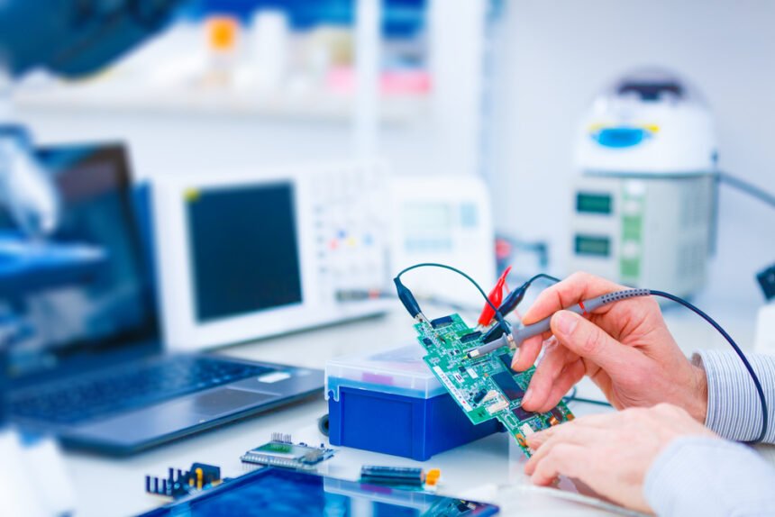
Most medical device companies value quality, safety, and predictability to maximize performance and minimize cost. Some of the many challenging production and performance issues can be minimized with proper cleaning of the PCB and mechanical assemblies used in these systems. Cleaning is very key for PCB as smaller, more densely populated circuit boards become a standard feature in the medical electronics industry. Without it, devices will not function as they should and will not withstand the rigorous regulation exercise put in place by governing bodies.


Mission-critical cleaning methods
The computing ability and functionality of modern medical devices is directly dependent on the processing power of the PCBs within them. That power is the result of smaller and more densely populated PCBs that are hard to clean. Better and quality cleaning prompts engineers to specify stronger, more active fluxes, which results in proper and better solder joints. This is because, failing solder joints causes huge damages to PCB software, and thus cleaning is essential to their functionality. Therefore proper cleaning implies better PCBs, which translate to effective and efficient medical electronics.
In addressing the cleaning challenges for medical electronics, the following methods have been deployed;
Vapor degreasing processes
Basically, it has two components; a specially designed low boiling nonflammable solvent and a specially designed cleaning machine. Externally, vapor degreasing systems are comprised of a top-loading and cleaning machine composed of two chambers namely: the rinse sump and the boil sump. Solvents with low boiling points are used as a cleaning agent, thus using much less electricity to clean. Also, these fluids have quite a lower viscosity, and lower surface tension than water thus can easily clean every part, including the smallest parts. Therefore this invention in the PCB design has facilitated cleanliness in medical electronics.
Solvent cleaning
Cleanliness is very key in a medical set up, going by the fact that medical electronics are complex, it requires liquids with low viscosity and surface tension ratings of solvent. It offers a new option for new design engineers, by ensuring that in the cleaning process, contaminated PCBs are not the cause of any failure and that better ones are built and distributed.


